
Commercialization of Ultra-High-Purity Colloidal Silica for State-of-the-Art Semiconductors —New production facilities to be established at Kyushu Plant (Fukuoka Area)—
August 19, 2026
Mitsubishi Chemical Corporation (Head Office: Chiyoda-ku, Tokyo; President: Manabu Chikumoto; hereinafter “the Company”) hereby announces that it has decided to commercialize ultra-high-purity colloidal silica (hereinafter “the Product”) for use as a raw material for polishing agents in cutting-edge semiconductors. The Company plans to establish new production facilities at its Kyushu Plant (Fukuoka Area) in Kitakyushu City, Fukuoka Prefecture, and begin commercial operations there in October 2028.
Colloidal silica is used as a raw material for surface polishing agents for silicon wafers and as a raw material for chemical mechanical polishing (CMP) slurries used on the interconnect layers of silicon wafers. When polishing the wiring layers of silicon wafers, it is necessary to achieve high material removal rates while simultaneously flattening the surface at the nanoscale, ensuring the absence of impurities, and minimizing scratches as much as possible; the appropriate shape and physical properties of colloidal silica particles vary depending on the material being polished.
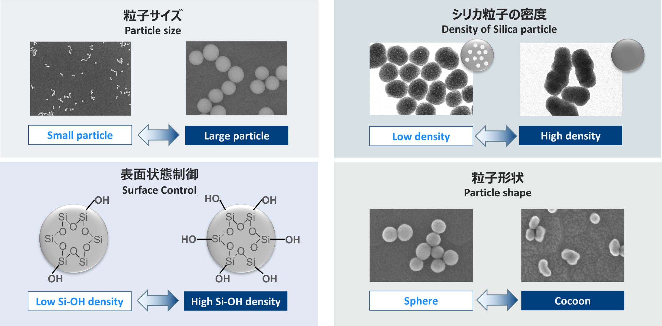
The ultra-high-purity colloidal silica that the Company is newly commercializing is produced through an integrated manufacturing process using an ultra-high-purity raw material (tetramethoxysilane) that minimizes impurity content. Drawing on advanced technical expertise cultivated over many years, parameters such as particle size and density can be customized to meet customers’ needs.
The semiconductor market is expected to see further growth, particularly in cutting-edge sectors such as generative AI and data centers. In its management vision “KAITEKI Vision 35,” the Company has identified “Enable advanced data processing and telecommunications” as one of its key business focus areas, and accordingly it will provide materials essential to cutting-edge semiconductor manufacturing worldwide and contribute to the materials supply chain that supports the advancement of semiconductors.
Colloidal silica is used as a raw material for surface polishing agents for silicon wafers and as a raw material for chemical mechanical polishing (CMP) slurries used on the interconnect layers of silicon wafers. When polishing the wiring layers of silicon wafers, it is necessary to achieve high material removal rates while simultaneously flattening the surface at the nanoscale, ensuring the absence of impurities, and minimizing scratches as much as possible; the appropriate shape and physical properties of colloidal silica particles vary depending on the material being polished.
The ultra-high-purity colloidal silica that the Company is newly commercializing is produced through an integrated manufacturing process using an ultra-high-purity raw material (tetramethoxysilane) that minimizes impurity content. Drawing on advanced technical expertise cultivated over many years, parameters such as particle size and density can be customized to meet customers’ needs.
The ultra-high-purity colloidal silica, customizable to customer needs
The semiconductor market is expected to see further growth, particularly in cutting-edge sectors such as generative AI and data centers. In its management vision “KAITEKI Vision 35,” the Company has identified “Enable advanced data processing and telecommunications” as one of its key business focus areas, and accordingly it will provide materials essential to cutting-edge semiconductor manufacturing worldwide and contribute to the materials supply chain that supports the advancement of semiconductors.
