
Semiconductors
Material Solutions Driving Miniaturization and Energy Efficiency
10/30/26
/ TEXT BY MCG
*The information, in this interview reflect the status at the time of the interview.
Semiconductors power every aspect of modern infrastructure, from smartphones to data centers. Today, the miniaturization of semiconductors is approaching the physical limit of atomic-level. To support this ongoing evolution, Mitsubishi Chemical (MCC) develops and supplies a wide range of advanced materials including EUV dry resist precursors essential for semiconductor manufacturing and gallium nitride (GaN) substrates for next-generation power electronics.
Semiconductors support virtually every modern industry
Semiconductors sit at the heart of almost all modern technology, from everyday items like smartphones and flat-screen TVs to hybrid and electric vehicles, as well as the data centers that perform the massive computations required for generative AI.
By definition, a semiconductor is a material that can both conduct and insulate electricity. Leveraging this unique property makes it possible to control electrical current, enabling fundamental information-processing functions such as switching, signal amplification, and data storage. Billions to hundreds of billions of nanoscale circuits (where one nanometer is a billionth of a meter) are etched onto a single chip no larger than a fingernail, serving as the indispensable brain behind modern infrastructure.
From a single wafer to a finished chip
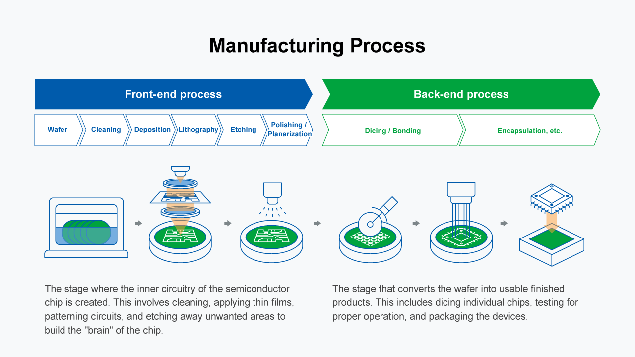
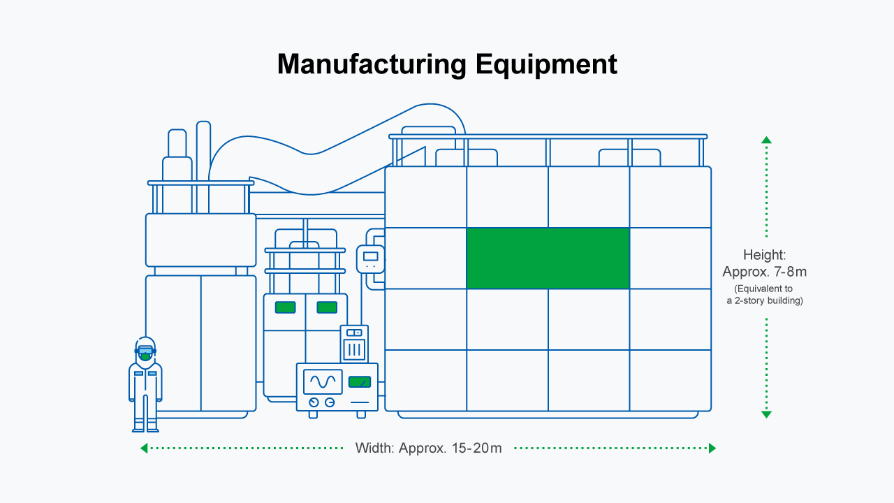
Manufacturing a semiconductor chip involves over a thousand precise steps, broadly divided into front-end processing (circuit fabrication) and back-end processing (assembly and chip protection). Some of the production equipment can be as tall as a two-story building (see Figure: Manufacturing Equipment). The MCC Group provides not only high-performance materials essential for semiconductor manufacturing but also materials used in semiconductor manufacturing equipment. In addition, the Group offers a wide range of supporting services, including precision cleaning, ultrapure water and wastewater treatment, chemical supply systems, and equipment maintenance. Through these products and services, the MCC Group helps enable higher-performance and increasingly miniaturized semiconductors.
Why do semiconductors keep evolving?
The continuous evolution of semiconductors is driven by the need to deliver higher performance while reducing power consumption. This evolution can be clearly understood by looking at three aspects: density, structure, and precision.
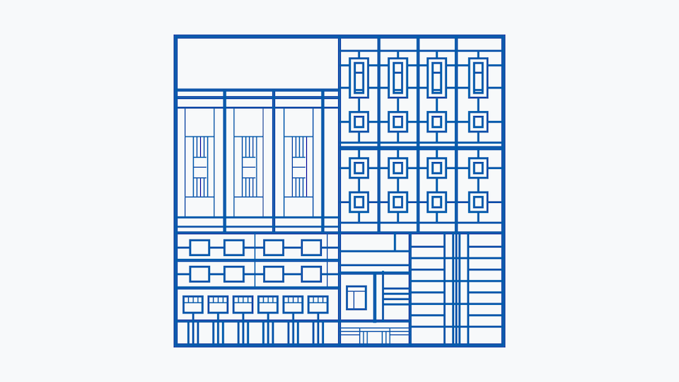
Density (Miniaturization): Patterning finer circuits allows more transistors to fit onto a chip of the same area, boosting overall processing power.
Structure (Structural changes): Long wiring distances create signal delays and power loss as heat. Placing chips as close together as possible and shortening interconnects (such as through 3D stacking and HBM) delivers both faster operation and better energy efficiency.
Precision (Alignment): Patterning circuits at the nanometer scale requires extremely precise control of exposure wavelengths and material deformation.
However, traditional technical approaches to advancing density, structure, and precision are now confronting hard physical and material limits:
● Physical Limits: Circuit feature sizes have reached the 1nm scale, approaching the dimensions of individual atoms, which are roughly 0.1 to 0.5nm. Further miniaturization is therefore becoming increasingly challenging.
● Material Limits: As chips pack in more circuits and handle higher data transfer rates, thermal management becomes a critical bottleneck. For example, standard PC CPUs built on 3nm to 7nm nodes can reach temperatures above 100°C, making advanced cooling technologies increasingly important.
MCC’s initiatives in advanced material development
Overcoming these challenges facing semiconductor advancement requires not only incremental improvements in existing technologies but also the development of new materials technologies.
MCC is developing advanced materials for next-generation semiconductor applications, including technologies related to miniaturization and power efficiency.
EUV dry resist precursors: Pushing the boundaries of miniaturization Improving semiconductor performance requires techniques that pattern circuits with finer resolution and higher accuracy. The industry currently relies primarily on wet processes, where liquid resist materials are coated onto wafers to form circuits. However, with growing demand for even finer circuit miniaturization, the industry needs new materials and processes that can support even higher resolutions.
EUV dry resist technology has emerged as a promising answer. Unlike wet resists, dry resist technology forms a film on the wafer via chemical reactions using vapor-phase precursors. Because film thickness and composition can be controlled with high precision, this approach is expected to enable finer, more accurate circuit patterning. These characteristics have drawn significant attention to dry resist as a key technology for advancing EUV lithography toward higher resolution and smaller circuit feature sizes.
The vapor-phase raw materials used to deposit these thin films are the EUV dry resist precursors supplied by MCC. Through the development of advanced precursor materials, MCC is contributing to the realization of next-generation semiconductor manufacturing technologies.
GaN (Gallium Nitride) substrates: The other key player in power efficiency Another major challenge in semiconductor evolution is power management. With the rapid adoption of generative AI driving up energy consumption in data centers, curbing power loss has become a top priority.
Consequently, gallium nitride (GaN) is gaining traction as a successor to conventional silicon (Si) for power semiconductors.
Compared with conventional silicon-based technologies, GaN may offer advantages such as higher voltage tolerance and faster switching characteristics, depending on device design and application requirements. A crucial factor supporting GaN devices is the crystal quality of the underlying substrate. Microscopic defects within the crystal structure can cause leakage currents and excess heat, negatively affecting device durability.
Leveraging years of expertise in ammonothermal growth technology (such as its proprietary SCAAT™-LP process), MCC is working to commercialize high-quality, large-diameter 6- to 8-inch GaN substrates for advanced power semiconductor applications.
Pioneering the future of semiconductors through chemistry
The evolution of semiconductors depends not only on advancements in circuit design and lithography equipment, but also fundamentally on innovation in materials science.
MCC offers a comprehensive lineup of materials and solutions supporting key stages of semiconductor manufacturing, from synthetic quartz powder and resist polymers in front-end processing to epoxy encapsulants in back-end processing, as well as EUV dry resist materials and GaN substrates. By leveraging cross-divisional and cross-company collaboration within the Group, MCC takes a holistic approach to the entire manufacturing process to deliver material solutions that address key challenges in yield improvement and next-generation device development. Under its management vision, "KAITEKI Vision 35," MCC highlights advanced data processing and communications as a strategic business focus area. Moving forward, MCC will continue to support the growth of the semiconductor industry through advanced material technology.
- Share


